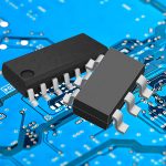
What is a switched mode power supply (SMPS)
A switched mode power supply (SMPS) designed for LED lighting applications is an LED driver that uses a switching regulator to convert the rectified DC power into a predetermined magnitude of DC power. SMPS LED drivers provide the most efficient and technically mature solution to LED current control. Today’s LED lighting products, in particular those designed for high end applications, place high demands on the driver’s ability to efficiently convert electrical power from an AC source to a DC load with outputs matched to the electrical characteristics of the LEDs. Despite the increasing cost and form factor restrictions in LED luminaire design, switched mode power supplies are still the most preferred type of power converters to drive high performance LED luminaires.
LED power requirements
An LED is a semiconductor diode that accepts only a forward voltage from a positively charged electrode to a negatively charged electrode. When the diode is forward biased the positive holes in the p-region and the negative electrons in the n-region recombine in the depletion zone (p-n junction) and release light. Most LED lights receive power input in AC form from the utility power grid. In the AC load the voltage varies sinusoidally between a positive and a negative value. When an LED is connected to the AC source directly, the electrical current flows through the p-n junction only when the amplitude of the AC waveform is positive. This means the LED will be switched on during each half cycle of the AC waveform and come with a dead time when it is not forward biased. A visible flicker will occur at a frequency of 100 Hz (for AC power with 50 Hz sinusoidal frequency) or at a frequency of 120 Hz (for AC power with 60 Hz sinusoidal frequency). In order for the LED to produce an uninterrupted output, a constant amount of forward current which is a DC current must be applied to the LED load. An LED is a low voltage device that works typically at 1.5 to 4.5 volt. Therefore the DC current rectified from the AC supply voltage must be regulated to match the LED load.
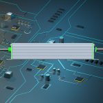
How does an SMPS LED driver work
An SMPS is typically an AC-DC LED driver but owes its name to the DC-DC switching converter that receives a rectified DC voltage and delivers a regulated DC output. The driver may include a rectifier, a ripple filter circuit, and a switching regulator. The rectifier is configured to convert (full-wave rectify) the alternating current in a direct current. The ripple filter circuit, which generally uses a capacitor at the rectifier output, is designed to smooth out the half sinewave humps, known as ripples, into a continuous DC voltage that resembles the smooth continuous voltage available from a battery. The rectified DC power is fed into the switching regulator for DC-to-DC conversion. This switching regulator provides a step−up or step−down function while trimming off unwanted peak voltage and maintaining a substantially constant output regardless of variations in load resistance and input voltage.
What is a switching regulator
As mentioned above, a switching regulator is basically a DC-DC converter. This voltage regulator uses one or more switching elements to transform the unregulated DC current into a pulsed waveform, which is then smoothed using an energy storage element. It typically comprises a semiconductor switch and an energy storage element which can be an inductance or a capacitance or a combination of both. The semiconductor switch is usually a power switch, such as a metal oxide semiconductor field effect transistor (MOSFET) or a bipolar junction transistor (BJT). The DC-DC converter regulates its output voltage by switching the power transistor between ON and OFF states at high frequencies. When the power transistor is in ‘ON’ mode the current in the capacitor or inductor ramps up and energy is stored. When the power transistor turns off this energy is released into the load.
The switching frequency or duty cycle is adjusted by a pulse-frequency-modulated (PFM) or pulse-width-modulated (PWM) controller which monitors the feedback control loop and fine-tune the frequency to compensate for output load variations and input voltage changes. The switching frequency is typically in the 50-400 kHz range which gives a fair trade-off between efficiency (switching losses), size and cost. A high switching frequency eliminates the need for a large inductor or capacitor, but increases the switching losses in the circuit. On the other side, the lower the switching frequency, the less the switching loss will occur, however this calls for a large inductor or capacitor.
SMPS topologies
Switched mode power supplies come in various topology options, including buck, boost, buck-boost, flyback, half-bridge, full bridge, forward converter, push-pull, etc. In addition to cost, efficiency and form factor considerations, the type of topology used very often depends on the features, e.g., input−to−output dielectric isolation, ripple filtering, multiple output capability, power factor, harmonics (noise), off line capabilities, dimming range, voltage and current stress across the power semiconductors, and input voltage placed across the primary transformer winding or inductor. Depending on the topology, the output from an SMPS may be regulated constant current or constant voltage.
The power switch in a switch-type converter is regulated by a control circuit based on variations of an input voltage, load resistance, and various internal parameters. Therefore, control methods will also need to be considered. The power conversion process of a switching power supply can be controlled using a variety of methods, including:
- Continuous conduction mode
- Voltage control with analog / digital compensator
- Discontinuous or boundary conduction mode
- Peak-current control
- Hysteretic current control
- Resonant control
- Constant on-time control
Buck
A buck circuit is a step-down converter that regulates input DC voltage down to a desired DC voltage for on−board regulator applications with output power less than 100 watts (although it’s capable of regulating over one kilowatt of output power). This simple type of DC-DC converter generally requires a single inductor and two semiconductor switches, either two MOSFETs, or a MOSFET and a diode. The buck circuit topology can be implemented using a number of current control methods, which include synchronous switching, hysteretic control, peak current control, and average current control. This type of topology is quite efficient (90–95%) and cost effective. The buck converter is very similar to a linear regulator, but it’s more preferable to a linear regulator for driving LED luminaires of which the input voltage is much higher than the output voltage. The load voltage of a buck-based driver must be no less than 85% of the supply voltage considering that the maximum duty cycle for reliable operation of a buck circuit is usually about 85%. A buck topology regulator allows for the best dynamic control of LED current and handles short to input and short to ground conditions well. The buck circuit topology does not offer isolation between the input and output circuits.
Boost
The boost converter is designed to drive an output that has a voltage at least 50% higher than the input. In boost circuits, a duty cycle less than 50% can lead to circuit damages caused by uncontrolled current. An inductor-based boost converter generally requires one inductor which must store enough energy to maintain the output current on the load for the entire switching period. These step-up converters are operated by a controller circuit in either continuous conduction mode (CCM) or discontinuous conduction mode (DCM). During an ‘ON’ cycle the load is disconnected from the inductor current, hence a large output capacitor is often required to maintain the current and help minimize EMI and the LED switching ripple (because the output current is a pulsed waveform). The large-output capacitor and the need for closed-loop control can complicate PWM dimming. The boost topology has 90-95% efficiency and low parts count. Boost regulators are typically used for board−level (i.e., non-isolated) step-up applications and should always be provided with overvoltage protection to survive damaging overvoltage transients.
Buck-boost
A buck-boost converter generates an output voltage that can be either higher or lower than the supply voltage. There are two variations of buck-boost topology: the single-ended primary inductance converter (SEPIC) and the Cuk converter. The SEPIC is a buck-boost converter with a low-side control switch in common with the boost regulator. This single-switch converter makes use of a capacitor to block any DC component between the input and output and thus provides non-inverted output coupling energy. A SEPIC circuit requires two identical inductors or a dual-winding inductor of which two windings wound on a common magnetic core to save circuit area. The Cuk converter is similar to a SEPIC except that it has an inverted output. Two inductors which operate in continuous conduction mode are wired in series with the input and the output, while the output inductor of a SEPIC circuit is connected to ground. This design automatically filters out high-frequency signals at the central node. The buck-boost topology also does not offer AC mains isolation.
Flyback
A flyback can be either isolated or non-isolated. A non-isolated flyback regulator is a DC-DC converter that uses an inductor with a single winding, which is basically buck-boost converter. An isolated flyback regulator uses two or three windings in the power inductor to provide galvanic isolation and enhanced safety. A flyback circuit is a discontinuous conduction mode converter which stores energy in the transformer while load current is supplied from an output filter capacitor. The ability to provide complete isolation between its input and output circuits makes flyback-based LED drivers a preferred choice for driving LED lamps and luminaires with metallic housing and for applications where a risk of electrical shock hazard may exist for the end users. The flyback transformer also provides energy storage and voltage scaling, allowing the regulator to easily generate multiple outputs with little investment in additional circuitry. The third winding, called a bootstrap or auxiliary winding, in a three-winding flyback is used to power the control IC. An optocoupler is commonly used to implement output voltage feedback. In practice a flyback converter is proven to deliver about 90% efficiency.
Why Use Switching Power Supplies?
The advantage of SMPS LED drivers is that they waste far less power and run much cooler than linear LED drivers, which simply throw away excess electric power as heat. In the switched mode of operation, the semiconductor switch has a very low resistance in its ‘ON’ state and therefore the voltage drop across its power path is minimal. High power conversion efficiency makes SMPS LED drivers particularly appeal to high power lighting applications which have tight limit on system efficiency and thermal loads. Switching power supplies are capable of producing a precise output voltage under varying input voltage conditions. This is a very attractive feature in the era of digital lighting as various lighting control applications such as tunable white lighting and RGB color mixing require accurate output regulation. Using topologies such as buck boost and flyback, SMPS LED drivers can accommodate a wide range of supply voltage, e.g. a universal input between 100V and 277V.
Disadvantages
A switching power supply is a considerably complex circuit that usually involves the use of inductors (or transformers), switching transistors, capacitors, associated control electronics. Complex compensation circuitry is often needed to maintain a stable output. The circuit can also generate greater current ripple that has to be smoothed out using capacitors. Not only the overall cost and volume of the LED driver is drastically increased, the complexity of the circuit can lead to compromised reliability. Electrolytic capacitors which can dry out when exposed to heat are the primary cause of failure in LED drivers. Since switching power supplies work in a high-frequency switch state, and a relative high level of electromagnetic interference (EMI) is inevitably generated. Accordingly, the electromagnetic compatibility (EMC) design of the LED power supply has become an additional challenge to be addressed.


Loading...