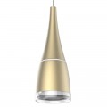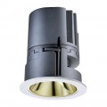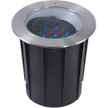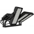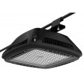

Light emitting diode (LED) is a junction diode produced by an epitaxial P-type layer and an epitaxial N-type layer on a heavily doped semiconductor compound base. LED has taken an ever more important place in the lighting area attributable to its advantages of high luminous efficacy, very low energy consumption, minimal radiation, etc. as opposed to traditional light sources. So that you can use an LED chip (die), the chip is typically encapsulated in a package that targets the light and that protects the chip from being damaged. A packaging process for chip packages is a very important part of forming electronic products. The LED packages shield the LED chips from the environment, offer the chips with protection from environmental contaminants, and allow the LED chips to interface electrically and thermally with printed circuit boards. Aside from that, LED packages provide mechanical support, allow the acceptable electrical connections (for example with the aid of "vias" through the package or bonding wires), help with heat dissipation, and improve the light emission efficiency from the LED chip. The package form of LED varies according to the application scenario, the appearance, the size, the heat dissipation solution, and the light emitting effect.
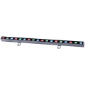
LED chips can generally be categorized into three types by structure, i.e., standard LED chip, inverted LED chip and vertical LED chip. LEDs can include horizontal LEDs and vertical LEDs. A vertical LED has better current dispersion performance compared to a horizontal LED. A vertical LED may have a superiorcurrent spreading performance owing to a structure in which a p-type semiconductor layer is placed at a lower portion in the vertical LED when compared to a conventional horizontal LED, and may have an outstanding heat dissipation performance by making use of a support substrate having a thermal conductivity superior to that of the sapphire substrate. Furthermore, the horizontal LED works with a growth substrate, say for example sapphire substrate, as a support substrate, whilst the vertical LED uses a substrate, for instance a metal substrate with a high thermal conductivity, and has superb heat emission performance. Typical package of LED light source includes lead package, surface mount (SMD) package and chip on board (COB) package. The LED packaging structure of surface mounted type has developed into a major form of package on account of the features of application convenience and small volume. In COB LEDs, LED chips are directly mounted to a substrate through die bonding and electrically connected through wire bonding. COB technology is a versatile packaging technology, which enables the use of a number of construction and connection materials. Chip-on-board LED packages make it possible for bright, uniform light output. These packages typically have a low thermal resistance which allows low junction temperatures at the chip level, in so doing resulting in increased efficiencies.
In standard packaging process of LEDs, the LED die is attached to the substrate by wire bonding, flip chip bonding, or eutectic bonding. Frequently, an LED package includes a substrate, an LED die assembled on the substrate, and an encapsulation formed on the substrate to cover the LED die. During a packaging process of the LED package, the LED die is wire bonded to electrical structures on the substrate by wires firstly, after which it is coated by the encapsulation that is generally applied to the LED die and the wires by a compression molding. In the wire bonding, gold wires are employed to electrically connect the electrodes of the LED die and the substrate. In most cases, wire bonds are utilized to apply a bias across the doped layers, injecting holes and electrons into the active layer where they recombine to emit light. Light is emitted from the active layer and from all surfaces of the LED. Wire bonding, nevertheless, has several drawbacks. For instance, wire bonds require a substantial amount of physical space. This could be problematic in miniaturized applications and applications. Furthermore, wire bond formation is a complicated process requiring time on expensive equipment. In eutectic bonding, eutectic alloy such as AuSn or SnPd is employed to electrically connect the electrodes of the LED and the substrate. Eutectic bonding posseses an advantage in which the alloy between the wafers is once liquefies during eutectic bonding, which allows hassle-free bonding even in the case where the wafers have somewhat irregular surfaces. Unfortunately, the eutectic bonding process is accomplished by heating. In the heating process, the light-emitting diode chip may easily shift or rotate, ultimately causing thermal damage to the electrodes disposed on the wafer and/or degradation of electrical contact between the semiconductor stacked layer structure and the electrodes. In the case where SnPd which allows bonding of a low temperature is applied, thermal damage may be sidestepped during the bonding. Even so, the eutectic portion can be re-liquefied at a low temperature, which can reduce the reliability of the bonding under circumstances where a heat is applied after manufacture of the LED.
The flip chip bonding technology is renowned for its characteristics of cutting down the size of chip package. In the flip chip bonding, solder balls of the LED die which are adhered to the electrodes of the LED die are placed facing the substrate and electrically coupled to the electrodes formed on the substrate by a reflow process. Flip chip LEDs are desirable in many different applications for the reason that do not use wire bonding. Both electrodes are positioned on a bottom surface of the LED for direct bonding to metal pads on a submount. Bonding may be completed by ultrasonic bonding, solder, conductive adhesive, or other methods. Light exits the surface of the LED opposite the electrodes. By virtue that the above flip-chip technology can make the chip connect directly with the connecting pins of the positive and the negative electric electrodes, this actually also has a bonus of rapid heat conducting and scattering, and thus is very desirable to be employed on high power LED components.
As LED packages are made smaller and slimmer, there is an endeavor to save costs of process and investment by upgrading existing WL ("Wafer Level") to CS ("Chip Scale"). Wafer level Packaging (WLP) is a process for packaging a die, chip, integrated circuit (IC) or other semiconductor device by making use of wafer level processing approaches to fabricate a plurality of packages in each wafer then separate the individual packages. Wafer level packaging is different from chip level packaging for the reason that WLP process is applied to a plurality of packages concurrently on a wafer or wafers while chip level packaging processes are applied to each chip or package individually. Wafer scale processing is efficient. But nevertheless, the submount wafer or other supporting layer that mechanically supports the thin brittle LED die adds cost. Moreover, the singulation process for typical supporting layers, for example ceramic or metal, is very complex in an effort to avoid breakage, metal burrs, and other problems. Chip level packaging can occur on wafers, getting rid of the separate step of having manufactured LEDs undergo a packaging line (packaging can sometimes be 60% of the total cost).
A chip-scale package (CSP) denotes a package for the light emitting device that is mounted on the semiconductor light emitting device structure in a wafer-scale process. When it comes to packaging technique by flip-chip bonding, chip-scale packaged LED device has been developed for the intention of miniaturization. A CSP (Chip Scale Package) may be accomplished which has a light-emitting device reduced in size (particularly, size in planar view from a direction perpendicular to a mounting substrate) to a level closer to a chip size of light-emitting elements. CSP technology drastically scales down the size of a conventional LED package by integrating sophisticated flip chip technology with phosphor coating technology. This removes metal wires and plastic molds for more versatile and compact designs and lowers costs. CSP products make it possible for flexibility in changing the size of the light-emitting surface and luminance level to address a broader base of lighting application requirements.